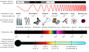
The nanometre (international spelling as used by the International Bureau of Weights and Measures; SI symbol: nm), or nanometer (American spelling), is...
5 KB (431 words) - 11:50, 31 August 2024
2 nm process (redirect from 2 nanometre process)
In semiconductor manufacturing, the 2 nm process is the next MOSFET (metal–oxide–semiconductor field-effect transistor) die shrink after the 3 nm process...
30 KB (2,500 words) - 19:50, 13 September 2024
350 nm process (redirect from 350 nanometre)
The 350 nanometer process (350 nm process) is a level of semiconductor process technology that was reached in the 1995–1996 timeframe by leading semiconductor...
3 KB (208 words) - 05:23, 7 February 2024
800 nm process (redirect from 800 nanometre)
The 800 nm process (800 nanometer process) is a level of semiconductor process technology that was reached in the 1987–1990 timeframe, by companies, such...
2 KB (173 words) - 18:13, 1 June 2024
32 nm process (redirect from 32 nanometre)
"45 nm" process in CMOS (MOSFET) semiconductor device fabrication. "32-nanometre" refers to the average half-pitch (i.e., half the distance between identical...
12 KB (1,213 words) - 22:04, 25 April 2024
22 nm process (redirect from 22 nanometre)
possibly disturbing Moore's law. The 20-nanometre node is an intermediate half-node die shrink based on the 22-nanometre process. TSMC began mass production...
8 KB (801 words) - 00:51, 28 February 2024
250 nm process (redirect from 250 nanometre)
The 250 nm process (250 nanometer process or 0.25 μm process) is a level of semiconductor process technology that was reached by most manufacturers in...
1 KB (102 words) - 02:29, 11 February 2024
180 nm process (redirect from 180 nanometre)
The 180 nm process is a MOSFET (CMOS) semiconductor process technology that was commercialized around the 1998–2000 timeframe by leading semiconductor...
4 KB (350 words) - 01:50, 1 December 2023
14 nm process (redirect from 14 nanometre)
December 2007, Toshiba demonstrated a prototype memory unit that used 15-nanometre thin lines. In December 2009, National Nano Device Laboratories, owned...
32 KB (2,767 words) - 20:03, 25 August 2024